


 수량을 선택해주세요.


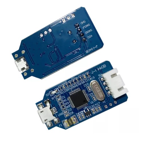
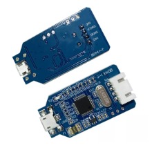
J-Link OB 디버거 V8 -SWD
(J-Link Debugger V8)

개요
- 본 제품은 J-Link OB 디버거 V8입니다.
- J-Link 온보드 디버거로 USB 연결을 통해 PC와 통신하며, SWD을 통해 타켓 장치와 통신합니다.
- SWD 인터페이스를 통해 디버깅 및 다운로딩 작업이 가능합니다. JTAG은 지원하지 않습니다.
특징
-
Supported kernels
All with SWD interface ARM7911, Cortex-M0M1M2M3M4A5A8A9 and other embedded MCU series.
Support MCU producer
ST(Stmicroelectronics), Freecale(Freescale), Nuvoton (New Tang), NXP(NXP), TI(Texas Instruments)
Cypress, Atmel, Analog, Fujitsu, Toshiba
Energy Micro, etc.
The connection method
SWD mode
Function and performance
Programming function: can burn FLASH ROM, EEPROM, AFR and so on.
Simulation function: support full speed running, single step debugging, breakpoint debugging and other debugging methods, you can view IO status, variable data and so on.
Programming performance: USB2.0 interface, SWD download, download fast!
Simulation performance: USB2.0 interface for simulation debugging, single step debugging, breakpoint debugging, fast response!
-
1, simplified interface, using 4-line SWD interface: VCC, SWDIO, SWCLK, GND, high-speed download simulation.
2, compatible with the traditional V8 simulator, the function is completely consistent.
3, the use of universal micro USB interface, easy to use (common Android phone universal interface).
4, support 3.3V output, maximum output 300MA current, convenient for users to debug and download the target board.
5, the new onboard self-recovery fuse, effective short circuit protection, debugging more safe.
6, ESD protection device, more stable.
7, transparent heat shrinkable tube packaging.
8, the firmware is stable, can be automatically upgraded, there will be no firmware damage phenomenon (full function V8 firmware problems).
9, U disk size, convenient engineering is to carry on business trips.
-
Interface description:
VCC(=3.3V),GND,SWDIO(=TMS=DIO),SWCLK(=TCK=CLK)
문서
- Data link: https://pan.baidu.com/s/1RdSbtvFxqKC7f9Is-Bq9Sg extraction code: 5 KSV
연관제품
- 연관제품 1