


 수량을 선택해주세요.


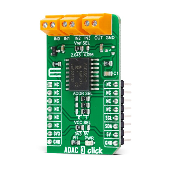
ADC/DAC 모듈 -PCF8591
(ADAC 3 CLICK)
개요
- 본 제품은 ADC/DAC 모듈 -PCF8591 입니다.
- PCF8591 칩을 기반으로 디자인된 제품으로 ADC 및 DAC 가 결합된 제품입니다.
- I2C 인터페이스를 가지고 있으며, 솔더 점퍼로 설정하여 3.3V 및 5V 시스템과 사용이 가능합니다.
특징
-
ADAC 3 Click as its foundation uses the PCF8591, a low-power CMOS data acquisition device from NXP Semiconductors. The PCF8591 comes with four analog inputs configurable as single-ended or differential inputs used to measure voltages, alongside one analog output representing an 8-bit digital-to-analog converter. In addition to measuring voltage, the user can create them as desired and even use DAC and ADC together to generate an input to a circuit and measure the results with the ADC, making it suitable for various control, monitoring, or measurement applications. By its internal structure, the PCF8591 also consists of an analog input multiplexing circuit, an on-chip track and hold function, alongside a serial interface block.
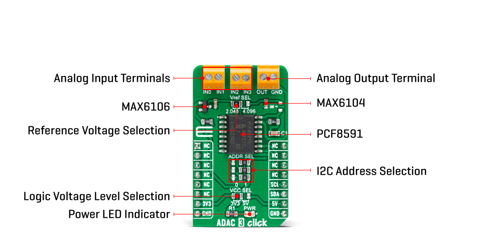
This Click board™ communicates with MCU using the standard I2C 2-Wire interface with a maximum clock frequency of 100kHz. The PCF8591 has a 7-bit slave address with the first four MSBs fixed to 1001. The address pins A0, A1, and A2, are programmed by the user and determine the value of the last three LSBs of the slave address, which can be selected by positioning onboard SMD jumpers labeled as ADDR SEL to an appropriate position marked as 0 or 1.
Besides, the user can choose the PCF8591 reference voltage value by positioning the SMD jumper labeled VREF SEL to a proper position, choosing between 2,048 and 4,096V provided by MAX6104 and MAX6106.
This Click board™ can operate with both 3.3V and 5V logic voltage levels selected via the VCC SEL jumper. This way, it is allowed for both 3.3V and 5V capable MCUs to use the communication lines properly. However, the Click board™ comes equipped with a library containing easy-to-use functions and an example code that can be used, as a reference, for further development.
SPECIFICATIONS
Type ADC-DAC Applications Can be used for various control, monitoring, or measurement applications On-board modules PCF8591 - low-power CMOS data acquisition device from NXP Semiconductors Key Features Low power consumption, combo solution with four analog inputs and one analog output, 8-bit successive approximation A/D conversion, I2C serial interface, analog inputs configurable as single ended or differential inputs, on-chip track and hold circuit, and more Interface I2C Compatibility mikroBUS Click board size M (42.9 x 25.4 mm) Input Voltage 3.3V or 5V
문서
연관제품
- 연관제품 1