


 수량을 선택해주세요.


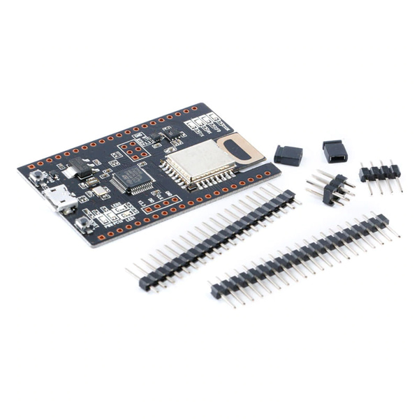
NodeMCU-BU01 보드 -UWB 트랜시버 실내 위치 추적 모듈, RTLS
(UWB Transceiver NodeMCU-BU01 Board)
개요
- 본 제품은 NodeMCU-BU01 보드 -UWB 트랜시버 실내 위치 추적 모듈, RTLS입니다.
- DecaWave DW1000칩 기반으로 디자인된 UWB BU-01 모듈과 MCU를 장착하고 있는 제품입니다.
- UWB 기술을 이용하여 실내에서 위치를 알아내고자 할 경우 사용할 수 있는 제품입니다.
- AT 명령을 이용하여 모듈을 제어합니다.
특징
- Antenna form: onboard PCB antenna
Frequency range: 3.5 GHz to 6.5 GHz
Interface: PWM/I2C/GPIO, all IO of MCU
Working temperature; -40℃ ~ 85 ℃
Storage environment: -40 ℃ ~ 125 ℃, <90%RH
Power supply range: 5V or 3.3V
Power consumption Development board backplane: 160mA (with MCU, sensor)
Product size: 35*55.5(±0.2)(W*H) mm - BU01
-
Simple integration, no RF design required
-
Using RTLS infrastructure to expand the communication range
-
Support high label density
-
Comply with IEEE 802.15.4-2011 UWB standard
-
Support 4 channels from 3.5 GHz to 6.5 GHz
-
Programmable transmit power
-
Power supply 2.8 V to 3.6 V
-
Power consumption in sleep mode<1mA
-
Support two-way ranging and TDOA
-
Support SPI interface
-
Data rate 110 kbps, 850 kbps, 6.8 Mbps
-
-

IO7: The default value is used as SYNC input. This pin can be reconfigured as a general-purpose I/O pin GPIO7 under software control.
IO6: General purpose I/O pin. At power-up, it is used as the SPIPHA (SPI phase selection) pin for configuring the SPI operating mode. After power-up, this pin will default to a general-purpose I/O pin.
IO5: General-purpose I/O pin. At power-up, it is used as the SPIPOL (SPI polarity selection) pin for configuring the SPI operating mode. After power-up, this pin will default to a general-purpose I/O pin.
IO4: General purpose I/O pin.
IRQ: Interrupt request output from DWM1000 to host processor and connected to PB0 of MCU. By default, IRQ is an active high output, but if necessary, it can be configured as active low. In order to operate correctly in SLEEP and DEEPSLEEP modes, it should be configured for active high operation. This pin will float in sleep and DEEPSLEEP states, unless it is pulled low, it may cause a spurious interrupt. When the IRQ function is not used, this pin can be reconfigured as the general-purpose I/O line GPIO8.
CLK: SPI clock and connected to PA5 of MCU
MISO: SPI data output and connect to PA6 of MCU
MOSI; SPI data input and connected to PA7 of MCU
CSN: SPI chip select and connect with PA4 of MCU. This is an active low enable input. A high-to-low transition on SPICSn indicates the start of a new SPI transaction. SPICSn can also be used as a wake-up signal to make DW1000 exit sleep or sleep state.
PA3: PA3 on MCU
PB1: PB1 on the MCU
PB10: PB10 on MCU
PB11: PB11 on MCU
LED1: PA2 on MCU, connect to LED1
LED2: PA1 on MCU, connect to LED2
BTN: PA0 on MCU, connect to BTN button
RESET: Reset pin on MCU, connected to reset button
GND: Ground
GND: Ground
V3.3: 3.3V power supply
V5 5V: power supply
V3.3: 3.3V power supply
GND: Ground
VBAT: MCU battery power supply Vbat
SCL: The SCL pin on the MCU, the default is to pull up 3.3V, and the sensor SCL pin is internally connected
SDA: SDA pin on MCU, 3.3V is pulled up by default, internal sensor SDA pin
PB8: PB8 on MCU
PB9: PB9 on MCU
PB5: PB5 on MCU
PB4: PB4 on the MCU
PB3: PB3 on the MCU
PA15: PA15 on MCU
V3.3: 3.3V power supply
RST: Reset pin on BU01 and connected to PB12 of MCU
WAKEUP: Wake-up pin on BU01 and connected to PB13 of MCU. When set to active high state, WAKEUP pin brings DW1000 from sleep or DEEPSLEEP state into working mode. If not used, this pin can be grounded
EXTON: The EXTON pin on BU01 is connected to PB14 of MCU, and the external device is enabled. Set during the wake-up process and remain active until the device enters sleep mode. Can be used to control external DC-DC converters or other circuits that are not needed when the device is in sleep mode to minimize power consumption
U1RX: UART1-RX on MCU
U1TX: UART1-TX on MCU
PA8: PA8 on MCU
PB15: PB15 on MCU
DIO: SWDIO pin on Swdio MCU, the default MCU programming pin
CLK: SWDIO pin on Swclk MCU, the default MCU programming pin
BT0: BOOT0 pin on BOOT0 MCU, which controls MCU startup mode
BT1: BOOT1 pin on BOOT1 MCU, which controls MCU startup mode
RESET: button RESET reset button BTN/PA0 button
BTN/PA0: Press the button to raise the PA0 pin
문서
- https://docs.ai-thinker.com/en/uwb%E6%A8%A1%E7%BB%84%E4%B8%93%E9%A2%982
- AT Command
- BU01 datasheet
-
Instructions for use:
The BOOT pin controls the startup mode: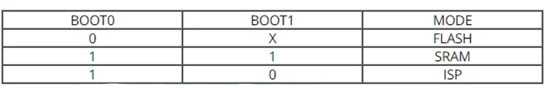 FAQQ1: How far can BU01-DB range measurement? How accurate is it?Answer: Point-to-point ranging 50m+ (related to placement and angular position), within 10CMQ2: How does BU01-DB work?Answer: Base station and tag mode, the base station will calculate and output the location information to the tagQ3: What can BU01-DB do besides ranging and positioning?Answer: In addition to positioning and ranging, it can also be used as a data transmission module to wirelessly forward device data.Q4: What is the use of STM32F103 on BU01-DB?Answer: STM32F103, as the main control chip, is responsible for carrying the algorithm driver code for running BU01.Q5: Can the temperature, humidity and acceleration sensors on the BU01-DB development board be used?Answer: Yes, the factory serial AT firmware has demo routines for temperature, humidity and acceleration acquisition.