


 수량을 선택해주세요.


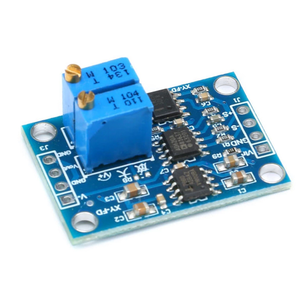
AD620 AC/DC 전압 신호 증폭 앰프 모듈
(AD620 High Accuracy Instrumentation Amplifier Module)
개요
- 본 제품은 AD620 AC/DC 전압 신호 증폭 앰프 모듈입니다.
- 1.5-10000배로 신호의 증폭이 가능하며, 높은 정확도, 낮은 오프셋을 가지고 있습니다.
- 제로값을 조절할수 있어 정확성을 높일 수 있습니다.
특징
- Wide input range This product adopts AD620 to amplify and can amplify microvolts and millivolts. Compared with LM358 on the market, it has high amplification precision and good linearity, and the maximum voltage output range is ±10V.
- Magnification The potentiometer is used to amplify the input signal, and the magnification is up to 1000 times, which can be adjusted only by a potentiometer.
- Adjustable zero point Adjust the zero point by adjusting the potentiometer, improve the accuracy, and there will be no zero drift phenomenon to meet customer needs.
- The negative voltage output module uses the 7660A negative voltage chip output negative voltage (-Vin), which can be supplied to customers to drive other dual power loads.
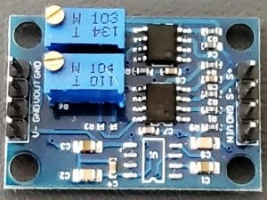
- The small size is 32*22mm, and four 3mm positioning holes are evenly distributed around the two sides, and the two rows are 2.54mm standard spacing.
- Input voltage: 3-12VDC
- Magnification: 1.5-1000 times adjustable, zero adjustable
- Signal input voltage: 100uV--300mV
- Signal output range: ± (Vin - 2V)
- Negative pressure output: greater than -Vin. Due to the internal resistance of the negative voltage chip output, the actual output is greater than -Vin, the greater the load power, the greater the negative pressure drop
- Offset voltage: 50μV
- Input bias current: 1.0nA (max)
- Common mode rejection ratio: 100dB
- Offset voltage drift: 0.6μV/°C (max)
- Stable, time: 2μV/month maximum
- Size: 32*22mm
- The output signal has small distortion, high frequency and noise filtering capability, and is more suitable for amplifying small signals.
문서
-
THEORY OF OPERATION:
The module mounts an AD620A Instrumentation Amplifier IC along with a 7660 Voltage Converter IC, LM358 Op Amp and assorted resistors and capacitors.
The module uses the AD620A version of the IC when referencing the data sheet.
Module Power
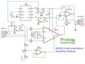
AD620 Instrumentation Amplifier Module Reverse Engineered Schematic
The module can be powered from 3.5 to 10V on the VIN pin and adjacent GND pin.
The VIN voltage passes through a 10 ohm resistor and connects to the +Vs pin on the AD620. We denote this as V+ on our reverse engineered schematic.
The 7660 voltage converter (charge pump) IC also takes in the V+ voltage and generates a negative voltage for the -Vs pin on the AD620 which we labeled as V-. This gives the AD620 both positive and negative power rails. V+ and V- also power the LM358 Op Amp
The negative voltage is also brought out to the pin labeled V- on the output side of the board in case you want to tap into it. Do not connect this V- pin to ground or another voltage or the 7660 will be damaged.
Module Amplification / Gain
The module accepts an AC or DC input signal of between 100uV and 300mV. The signal is input on the S+ and S- pins.
If the input is a ground referenced (single-ended) signal, the signal is connected to S+ and signal ground is connected to S-. Alternatively, a differential signal such as from a bridge sensor can be input across the S+ and S- pins.
The inputs have a 1K series resistor to limit input current to a safe level.
Gain of the AD620 is adjusted using a 100K potentiometer (marked 104). The advertised gain is 1.5x to 1000x and a lower resistance equals a higher gain. Turning the pot CW increases the gain.
The output of the AD620 is passed through one of the two LM358 op amps configured as a unity gain buffer. The LM358 can source about 30mA and sink 20mA. The output of this buffer is available on the pin labeled VOUT.
Zero Offset Adjustment
The other half of the LM358 is also setup as a unity gain buffer to feed the Vref input of the AD620.
The input of the LM358 has a 10K potentiometer (marked 103) and series 1K resistor tied between the V+ and V- power rails. The potentiometer adjusts the voltage input to the LM358 and the output is fed into the Vref pin on the AD620. This allows any offset to be adjusted out or if desired, a positive or negative offset can be adjusted in. Turning the potentiometer CW increases the offset in a positive direction.
To set the offset, the S+ and S- pins are shorted together and the 10K zero offset potentiometer is adjusted until the voltage at VOUT measures 0V or the desired amount of offset.
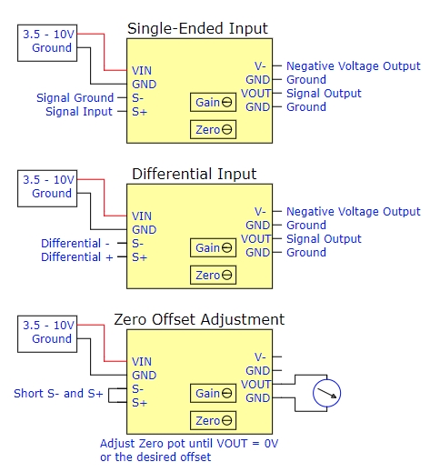
Module Connections
The module has inputs on one end and outputs on the other. These can be used to connect wires or header pins can be soldered in depending on the application.
1×4 Input Header
- VIN = Module power (3.5 to 10V)
- GND = Ground for module power
- S- = Signal Input (negative connection)
- S+ = Signal Input (positive connection)
1×4 Output Header
- V- = Negative voltage output from 7660
- GND = Ground
- VOUT = Signal Output
- GND = Ground
The diagrams below show the basic connection setups for single-ended and differential inputs as well as the setup for adjusting the Zero Offset.
OUR EVALUATION RESULTS:
These are interesting modules with good potential and will work as-is for many applications, but as shipped, the module has some limitations which can be significantly improved upon if achieving optimum performance is desired.
Ditch the 7660
AD620 module with 7660 Removed
The main weakness of the module is due to using the 7660 charge pump IC to generate the negative voltage.
Although this is convenient since it only requires one positive voltage to power the module, the electrical noise created by such a device creates more circuit noise than is desirable for an amplifier primarily designed to amplify very small signals. The 7660 is also subject to latch-up if it is driven at too high a voltage and so the module seems happiest in stock form when the VIN power is kept down around the 5V range.
If it is desired to get the best performance out of the module and you have a clean +/- power source such as from linear regulators, one easy hack is to simply remove the 7660 IC as shown to the right.
You can then feed the external negative voltage to the V- pin along with the positive voltage fed to the VIN pin as normal. This also allows you to run a higher power rail of up to ±15V based on the maximum limitation of the LM358 of ±16V. The 7660 can either be unsoldered or the pins simply clipped off. The other components can all remain in place.
The scope capture below is with the 7660 IC removed, power VIN and V- inputs set to ±12V and a 5mV 1kHz AC waveform input. The output maxes out at about 10.5V which gives a gain of 2000x. The small glitch was also present on the input signal.
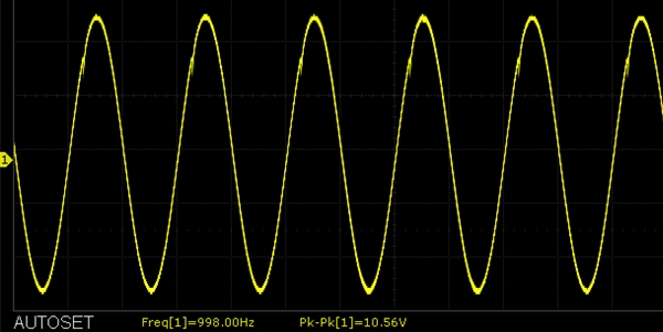
AD620 Instrumentation Amplifier Scope Capture 5mV 1kHz input
Consider Changing the 100K pot
The modules works well at lower gains, but at the highest gains, the resistance needed is approaching 50 ohms which is hard to get out of a 100K pot. If it is desired to work at higher gains, it would be beneficial to change the 100K pot to a smaller value one such as 10K or 1K to give better linearity at the lower end of the resistance range. We have gotten up to 2000x with the 100K pot in place, but the amplification adjustment is very coarse.
Alternatively, if a fixed gain is desired, the pot can be replaced with a fixed value resistor in location R3 (Rgain) which is currently unstuffed next to the 100K pot. There is also a stuffed location also labeled R3 which should be left alone.
The formula for calculating the resistor value is Rgain = 49.9K / (Gain – 1). For a fixed gain of 100x, the resistor value would be 49900 / (100-1) = 499 ohms. The data sheet has a table of commonly used value.
BEFORE THEY ARE SHIPPED, THESE MODULES ARE:
- Basic zero offset functionality tested and adjusted for 10x amplification using 200mV DC input.
- Packaged in a resealable ESD bag for protection and easy storage.
Notes:
- None
TECHNICAL SPECIFICATIONS
Operational Ratings Vcc Range 3.5-10V (VIN pin) Current Max Sink Current 20mA Max Source Current 30mA Bandwidth Gain = 100 120kHz Input Signal Range 100uV – 300mV Input Signal Type AC or DC Amplification Range 1.5 – 1000x Output Voltage Max VIN – 2V Offset Voltage Typical / Max 30uV / 125uV Input Bias Current Typical / Max 0.5nA / 2.0nA Offset Voltage Drift Max 1uV / degree Common Mode Rejection Ratio Gain = 10 100dB Dimensions PCB (L x W) 32 x 22mm (1.3 x 0.87″) Datasheet Analog Devices AD620