


 수량을 선택해주세요.


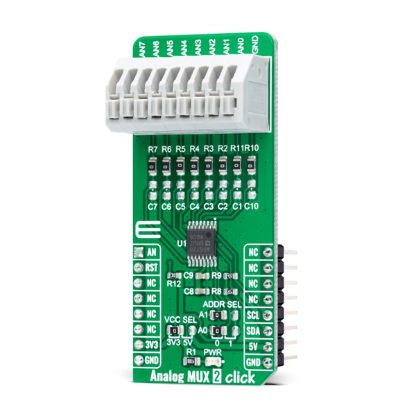
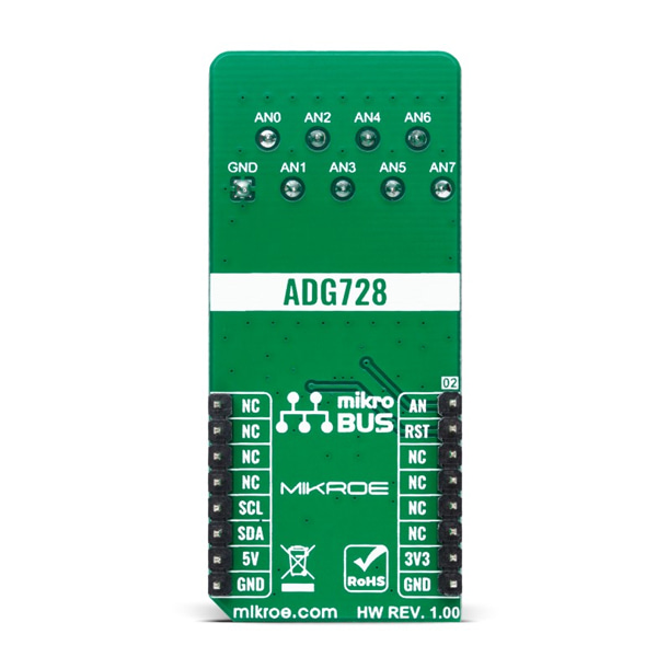
아날로그 멀티플렉서 -ADG728모듈
(ANALOG MUX 2 CLICK)
개요
- 본 제품은 아날로그 멀티플렉서 -ADG728모듈입니다.
- 8개의 입력중 하나를 선택하여 하나의 출력으로 내보내는 모듈로 ADG728 8 채널 아날로그 매트릭스 스위치를 기반으로 디자인된 제품입니다.
- 아날로그, I2C 인터페이스를 가지고 있습니다.
특징
-
Type Port expander Applications Can be used for a wide range of applications, from industrial and instrumentation to medical, consumer, communications, and automotive systems. On-board modules ADG728 - low voltage, CMOS 8-channel analog matrix switch with a serially controlled 2-wire interface from Analog Devices Key Features 8-to-1 matrix switch, low on-resistance, 'Break-Before-Make' switching action, serially controlled, and more. Interface Analog,I2C Compatibility mikroBUS Click board size L (57.15 x 25.4 mm) Input Voltage 3.3V or 5V -
Analog MUX 2 Click is based on the ADG728, a low voltage, CMOS 8-channel analog matrix switch with a serially controlled 2-wire interface from Analog Devices. The ADG728 can operate equally well as either multiplexer, demultiplexer, or switch array, providing more flexibility. It also features a low on-resistance closely matched between switches and very flat over the full signal range. During the Power-Up of the ADG728, all switching channels will be in the OFF condition, and the internal shift register will contain all zeros. All channels exhibit 'break-before-make' switching action preventing momentary shorting when switching channels.
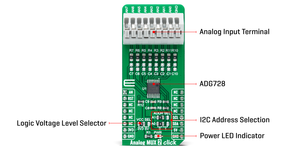
Each bit of the 8-bit serial word corresponds to one switch of the device. Internal switching channels are independently controlled by an individual bit, providing an option of having any, all, or none of the switches activated. All of the input channels of the multiplexer can be easily connected to a 9 pole spring action block terminal, without having to use any additional tools, such as screwdrivers, while the output pin from the multiplexer is routed to the AN pin on the mikroBUS™ socket.
Analog MUX 2 Click communicates with MCU using the standard I2C 2-Wire interface with a frequency of up to 400kHz. It also has two address pins (A0 and A1) programmed by the user to determine the value of the last two LSBs of the slave address, selected by onboard SMD jumpers labeled as ADDR SEL to an appropriate position marked as 0 and 1, allowing selection of the slave address LSBs. Also, this Click board™ has a Reset pin routed to the RST pin on the mikroBUS™ socket, which clears the input register and turns all switches to the OFF condition.
When changing the switch conditions, a new 8-bit word is written to the input shift register. The ADG728 compares the state of switches from the previous write cycle to minimize glitches on the switches output. This can be achieved if the switch is already in the ON condition and is required to stay ON.
This Click board™ is designed to operate with both 3.3V and 5V logic voltage levels selected via the VCC SEL jumper. It allows for both 3.3V and 5V capable MCUs to use the I2C communication lines properly. However, the Click board™ comes equipped with a library that contains functions and an example code that can be used, as a reference, for further development.