


 수량을 선택해주세요.


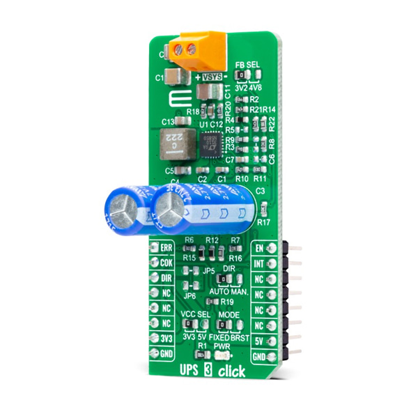
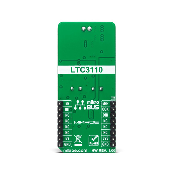
시스템 백업 슈퍼캐패시터 UPS 모듈 -LTC3110
(UPS 3 CLICK)
개요
- 본 제품은 시스템 백업 슈퍼캐패시터 UPS 모듈 -LTC3110입니다.
- 양방향 스텝다운 스텝업 DC-DC 레귤레이터/충전 기능의 LTC3110 칩을 기반으로 디자인된 제품으로 입력 전압을 스텝업 혹은 스텝다운하여 보드상의 슈퍼캐패시터를 충전합니다.
- backup 모드와 charge 모드의 2가지 모드로 동작하며, 백업 모드에서는 장착된 슈퍼캐패시터에서 1.8V-5.25V의 시스템 전압출력을 유지하며, 충전 모드에서는 외부전원을 이용하여 슈퍼패캐시터를 충전합니다.
특징
-
Type Battery charger Applications Can be used for a backup power source for a wide range of battery-operated embedded applications On-board modules LTC3110 - bidirectional buck-boost DC/DC regulator with capacitor charger and balancer from Analog Devices Key Features High accuracy, selectable switchover from Charge to Backup mode, low-noise switching frequency algorithm, high efficiency, ideally suited for backup applications, and more. Interface GPIO Compatibility mikroBUS Click board size L (57.15 x 25.4 mm) Input Voltage 3.3V or 5V -
UPS 3 Click as its foundation uses the LTC3110, a bidirectional buck-boost DC/DC regulator with capacitor charger and balancer from Analog Devices. The buck-boost regulator utilizes a proprietary switching algorithm that allows the system voltage to be regulated above, below, or equal to the voltage on the storage element without discontinuity in inductor current or large voltage ripple in the backup voltage. During charging, a limit for the average current drawn from the system power source is accurately programmed with an external resistor and set to 450mA. It also has an integrated, active voltage balancing buffer that prevents capacitor overvoltage conditions caused by capacitor mismatch while charging a stack of supercapacitors.
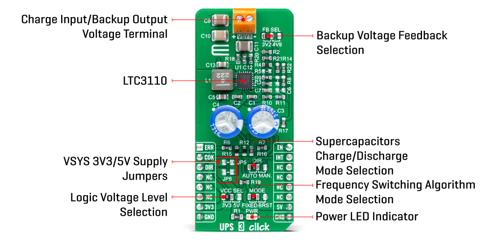
The LTC3110 operates in two modes, Backup and Charge mode. In Backup mode, the device maintains a system voltage of 1.8V to 5.25V, powered from the supercapacitor stored energy. This feature ensures that all usable stored supercapacitor energy is utilized, thereby extending backup times or shrinking the storage capacitors. In Charge mode, when the primary power system labeled as VSYS is active, the LTC3110 can independently or through user command reverse the direction of power flow using the regulated system voltage to charge and balance the supercapacitors. Also, this Click board™ uses Charge/Backup Mode Indicator, routed on the INT pin of the mikroBUS™ socket, that is pulled in a low logic state while the regulator is in Charge mode, or a high while the regulator is in Backup mode.
UPS 3 Click communicates with MCU using several GPIO pins. The EN pin, routed on the PWM pin of the mikroBUS™ socket, is used to put the LTC3110 into Normal operation mode or in a Shutdown. The LTC3110 includes a voltage comparator used to supervise voltage on the storage element associated with the ERR pin of the mikroBUS™ socket alongside a pin labeled as COK, routed on the RST pin of the mikroBUS™ socket, to indicate the energy storage element's charging state.
In addition to all these features, this Click board™ also has several selectable jumpers. One of them labeled as MODE offers to select between variable or fixed-frequency switching algorithm, Burst or PWM Mode, setting onboard SMD jumper to an appropriate position marked as FIXED and BURST. The other one labeled as FB SEL represents Backup Voltage Feedback Selection which offers the choice between 3.2V and 4.8V to set the voltage on the load when the supercapacitor discharges in Backup mode.
With the DIR pin routed on the CS pin of the mikroBUS™ socket, the LTC3110 can instantly reverse the inductor current and change between Charging and Backup operation modes, reacting quickly on a power failure condition by providing the backup voltage to the system. In combination with the jumper labeled as DIR, this pin allows automatic charging of the supercapacitor when a system voltage is present and works as a DC/DC converter providing system backup power to the load due to lack of system power. Otherwise, users have control overcharging and discharging the supercapacitor manually, changing the DIR pin's logic state.
This Click board™ can operate with both 3.3V and 5V logic voltage levels selected via the VCC SEL jumper or through SMD jumpers labeled as JP5 and JP6 through which the VSYS voltage powers up the mikroBUS™ 3.3V and 5V power rails. It allows for both 3.3V and 5V capable MCUs to use communication lines properly. However, the Click board™ comes equipped with a library containing easy-to-use functions and an example code that can be used, as a reference, for further development.