


 수량을 선택해주세요.


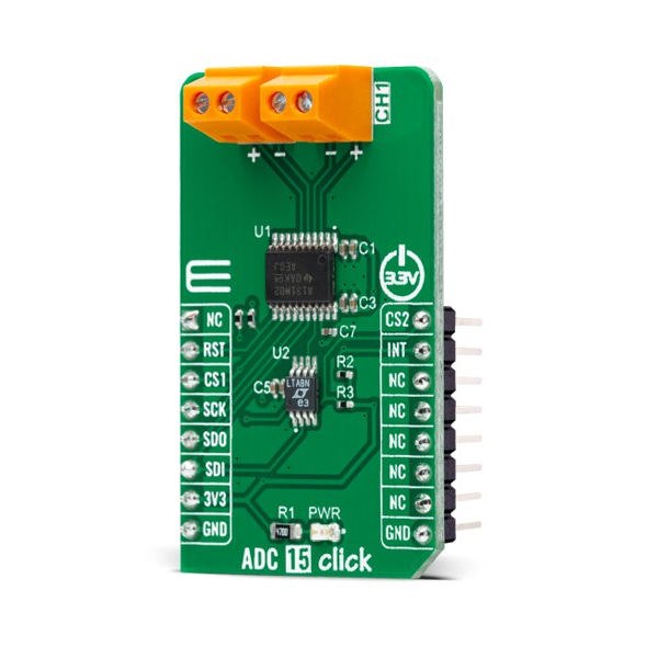
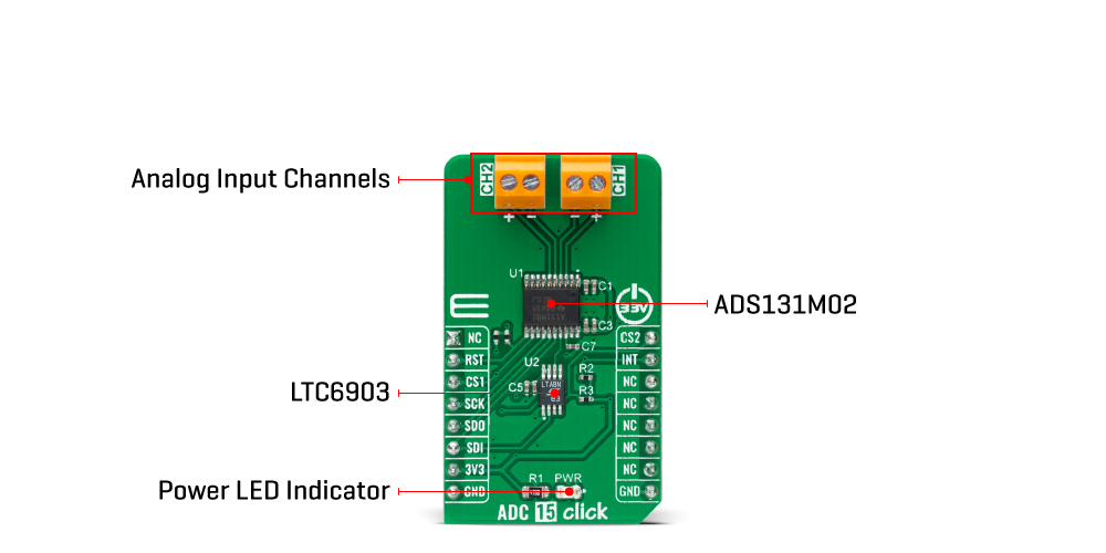
2채널 24비트 ADC 모듈 -ADS131M02
(ADC 15 CLICK)
개요
- 본 제품은 2채널 24비트 ADC 모듈 -ADS131M02입니다.
- 델타-시그마 아날로그 디지털 컨버터 ADS131M02 칩을 탑재하고 있습니다.
- 2개의 ADC의 입력은 SPI 인터페이스를 통해 개별적으로 설정이 가능합니다.
특징
-
HOW DOES IT WORK?
ADC 15 Click as its foundation uses the ADS131M02, a low-power, two-channel, simultaneously sampling, 24-bit, delta-sigma (ΔΣ) analog-to-digital converter (ADC) with a low-drift internal reference voltage from Texas Instruments. The dynamic range, size, feature set, and power consumption are optimized for cost-sensitive applications requiring simultaneous sampling. An integrated negative charge pump allows absolute input voltages as low as -1.3 V, which enables measurements of input signals varying around the ground with a single-ended power supply.
The ADS131M02 features a programmable gain amplifier (PGA) with gains up to 128. An integrated input pre-charge buffer enabled at gains greater than 4 ensures high input impedance at high PGA gain settings. The ADC receives its reference voltage from an integrated 1.2V reference, allowing differential input voltages as large as the reference. Each channel on the ADS131M02 contains a digital decimation filter that demodulates the output of the ΔΣ modulators. The filter enables data rates as high as 32 kSPS per channel in high-resolution mode. The relative phase of the samples can be configured between channels, thus allowing an accurate compensation for the sensor phase response. Offset and gain calibration registers can be programmed to adjust output samples for measured offset and gain errors automatically.
The ADC 15 Click communicates with MCU through a standard SPI interface to read the conversion data, configure and control the ADS131M02, supporting the most common SPI mode - SPI Mode 1. To normally run the ADS131M02, an LVCMOS clock must be continuously provided at the CLKIN pin, which is achieved with the LTC6903 programmable oscillator activated via the CS2 pin routed to the PWM pin on the mikroBUS™ socket. The frequency of the clock can be scaled in conjunction with the power mode to provide a trade-off between power consumption and dynamic range. Selection of the bits in the CLOCK register allows the device to be configured in one of three power modes: high-resolution (HR) mode, low-power (LP) mode, and very low-power (VLP) mode.
In addition, this Click board™ also uses features such as data-ready/interrupt routed to the INT pin on the mikroBUS™ socket, that serves as a flag to the host to indicate that new conversion data are available, and Reset routed to the RST pin that allows for a hardware device reset.
This Click board™ can be operated only with a 3.3V logic voltage level. The board must perform appropriate logic voltage level conversion before use with MCUs with different logic levels. However, the Click board™ comes equipped with a library containing functions and an example code that can be used, as a reference, for further development.
-
Type ADC Applications Can be used for energy metering, power metrology, and circuit breaker applications On-board modules ADS131M02 - low-power, two-channel, simultaneously sampling, 24-bit, delta-sigma (ΔΣ) analog-to-digital converter (ADC) with a low-drift internal reference voltage from Texas Instruments Key Features Two simultaneously sampling differential inputs, programmable gain and data rate, integrated negative charge pump allows input signals below ground, wide dynamic range, low power, and energy-measurement-specific features, and many more Interface SPI Compatibility mikroBUS Click board size M (42.9 x 25.4 mm) Input Voltage 3.3V