


 수량을 선택해주세요.


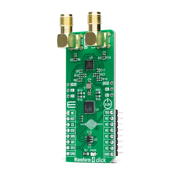
고성능 웨이브폼 DDS 신호생성기 모듈 -AD9106
(WAVEFORM 4 CLICK)
개요
- 본 제품은 고성능 웨이브폼 DDS 신호생성기 모듈 -AD9106 입니다.
- 4채널, 12비트, 180MPS 웨이브폼 생성기 AD9106 칩을 장착하고 있습니다.
- 칩내에 SRAM과 DDS(direct digital synthesis)를 내장하고 있습니다.
- SPI 인터페이스를 가지고 있으며, 3.3V 시스템과 사용이 가능합니다.
특징
-
HOW DOES IT WORK?
Waveform 4 Click as its foundation uses the AD9106, a high-performance, quad digital-to-analog converter (DAC) integrating on-chip pattern memory for complex waveform generation with a direct digital synthesizer (DDS) from Analog Devices. The DDS is a 12-bit output, up to 180 MHz master clock sinewave generator with a 24-bit tuning word allowing 10.8 Hz/LSB frequency resolution. This Click board™, by default, uses an onboard 125 MHz crystal oscillator as a clock source, which is also the maximum output frequency for this board. . The high-speed, high-dynamic-range, multichannel complex waveforms generated by AD9106 are suitable for applications such as ultrasound transducer excitation, medical instrumentation, portable instrumentation, signal generators, and arbitrary waveform generators.
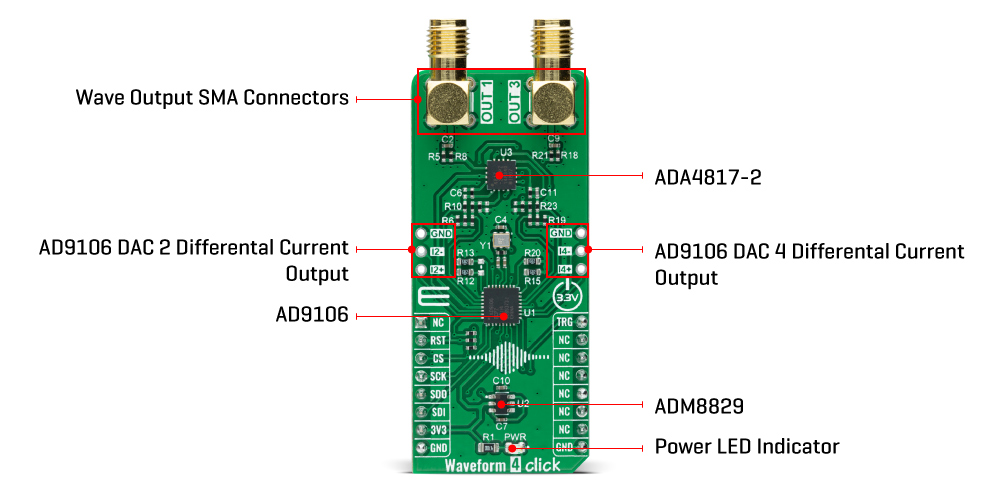
Pattern data can include directly generated SRAM-stored waveforms, DDS outputs amplitude-modulated by SRAM, or DDS frequency tuning words from SRAM providing chirp or frequency shift keying (FSK) modulation. An internal pattern-control state machine allows the user to program the pattern period for all D/A converters, the start delay within the pattern period for the signal output on each D/A converter channel, and the repetition rate of the pattern. The generation of a pattern is configurable via TRG routed to the PWM pin of the mikroBUS™ socket. A falling edge on the TRG pin starts generating a pattern, while the rising edge represents a request for the termination of pattern generation.
The AD9106 has a single frequency output and independent programmable phase shift outputs for each of the four integrated DACs. Besides, gain adjustment factors and offset adjustments are applied to the digital signals on their way into the four DACs. The two DAC outputs of the AD9106 are filtered by an RC network and then amplified via ADA4817-2, an operational amplifier that combines new architecture for FET input operational amplifiers with the eXFCB process from Analog Devices, resulting in an outstanding combination of speed and low noise. The other two outputs, without any amplification, were routed on onboard headers labeled as I2 and I4. In addition to the positive supply voltage requirement, the ADA4817-2 amplifier also has a negative supply voltage, achieved by the ADM8829, a charge-pump voltage inverter used to generate a negative supply from a positive input from Analog Devices.
The output signal from the ADA4817-2 follows two paths. One path is routed to an output connector labeled as OUT1, while the other path is routed to an output connector labeled as OUT3. On these connectors, the AD9106 can generate two types of signal patterns under the control of its programmable pattern generator: periodic pulse train waveforms that repeat indefinitely or periodic pulse train waveforms that repeat a finite number of times.
This Click board™ communicates with MCU through a standard SPI interface to program the internal registers for complete control of the AD9106. Besides, it possesses additional functionality such as a reset function implemented and routed at the RST pin of the mikroBUS™ socket, which resets all registers of the AD9106 to its default state.
This Click board™ can be operated only with a 3.3V logic voltage level. The board must perform appropriate logic voltage level conversion before use with MCUs with different logic levels. However, the Click board™ comes equipped with a library containing functions and an example code that can be used, as a reference, for further development.
-
Type Clock generator Applications Can be used as ultrasound transducer excitation, medical instrumentation, portable instrumentation, signal generators, and arbitrary waveform generators On-board modules AD9106 - high-performance, quad digital-to-analog converter (DAC) integrating on-chip pattern memory for complex waveform generation with a direct digital synthesizer (DDS) from Analog Devices Key Features Highly integrated quad DAC for complex waveform generation, on-chip 4096 × 12-bit pattern memory, 12-bit output DDS, low power consumption, high performance, and more Interface SPI Compatibility mikroBUS Click board size L (57.15 x 25.4 mm) Input Voltage 3.3V